
The Promise of Nanotechnology in Computing: Building the Computers of the Future
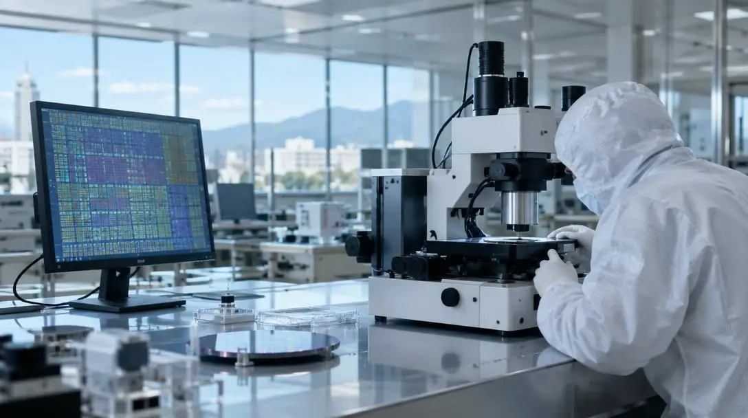
The relentless expansion of artificial intelligence, cloud infrastructure, and the Internet of Things has transformed computing into a vital utility that underpins modern communication, global industry, and daily personal routines. However, the silicon microchips that have fueled this digital revolution are colliding with the immovable laws of classical physics. As microprocessors are packed with billions of ever-smaller components, they encounter severe issues with electrical leakage, excessive thermal output, and compromised reliability.
To overcome these performance bottlenecks, researchers are looking beyond conventional silicon architecture toward nanotechnology. Operating at a scale measured in billionths of a meter, nanoscale engineering enables the manipulation of individual atoms and molecules to create computational devices that are smaller, faster, and substantially more energy-efficient than existing hardware. Exploring how matter behaves at this extreme frontier reveals how nanoscale systems will define the next generation of computing machines.
Key takeaways
- Nanotechnology operates between 1 and 100 nanometers, a scale where quantum effects and higher surface-area-to-volume ratios fundamentally alter material behavior.
- Traditional silicon transistors face hard physical boundaries, including gate leakage current, extreme heat dissipation, and diminishing reliability as components shrink to atomic thresholds.
- Breakthrough computing architectures rely on nanomaterials like nanowires, graphene, and biomolecules, alongside physical phenomena like electron spin, to dramatically elevate processing speed and data density.
- Successful implementation requires hybrid integration, pairing emerging nanoscale materials with legacy silicon microelectronics while navigating rigorous cleanroom fabrication protocols.
- Realizing the potential of nanoscale computing demands international collaboration on material safety, environmental lifecycle management, and standard characterization metrics.
Understanding the science of the nanoscale frontier
Nanotechnology refers to the design, synthesis, and application of materials and functional devices structured between 1 and 100 nanometers. To put this dimension into perspective, a single nanometer represents one-billionth of a meter. At this scale, matter ceases to behave strictly according to the intuitive rules of macroscopic classical physics. Instead, quantum mechanical principles take precedence, altering electrical conductivity, optical absorption, and chemical reactivity.
One of the primary drivers of this behavioral shift is the massive increase in the surface-area-to-volume ratio. As a bulk substance is divided into nanoscale particles, an exponentially higher percentage of its constituent atoms are exposed on its outer surface. This structural arrangement makes nanomaterials far more reactive and dynamic than their macroscopic counterparts. Outside of advanced computing, nanoscale materials are already woven into everyday consumer goods, such as antibacterial silver nanoparticles used in modern wound dressings and UV-blocking titanium dioxide nanoparticles integrated into topical sunscreens. These commercial implementations prove that atomic manipulation is an achievable engineering reality, laying the groundwork for re-engineering the building blocks of computing.
The physical limits of traditional silicon computing
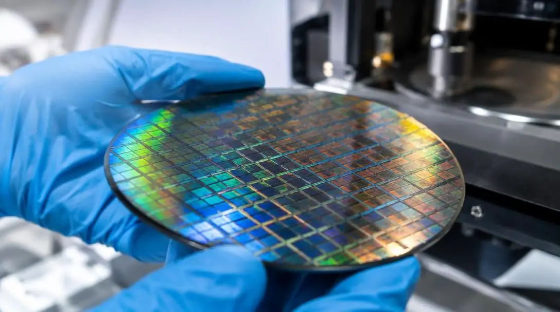
For more than half a century, the primary engine of technological expansion has been the steady miniaturization of the silicon field-effect transistor. In standard microprocessors, millions or billions of microscopic silicon switches act as binary gates, opening and closing to govern the passage of electrical currents that represent digital ones and zeros. Shrinking these gates historically allowed engineers to pack more computational power into smaller dies while lowering unit costs.
However, modern silicon manufacturing has reached an atomic impasse. When conductive channels shrink to a thickness of only a few atoms, the barrier separating electrical states breaks down:
- Leakage current: As the insulation layer on a transistor gate becomes impossibly thin, electrons escape from their designated pathways via quantum tunneling. This unintended drift drains battery reserves, generates false signals, and consumes standby power even when a processor is idle.
- Heat dissipation: Packing billions of leaking electrical switches into a chip the size of a fingernail creates an extreme thermal concentration. Dissipating this intense heat requires bulky cooling systems and power budgets that restrict the clock speeds of modern data centers.
- Reduced reliability: At near-atomic tolerances, minor structural defects, thermal expansion cycles, and electromigration can sever an internal trace, leading to permanent operational errors and shortened hardware lifespans.
As conventional silicon gates approach the width of a handful of atoms, the physical breakdowns of leakage current and excessive heat stall the continued advancement of traditional microprocessors.
Core nanoscale computing technologies in modern research
To break through the silicon bottleneck, laboratory researchers are building alternative computational systems that exploit novel molecular properties, subatomic forces, and light-based signaling. By replacing standard silicon traces with specialized nanoscale elements, developers can achieve unprecedented processing speeds and storage volumes.
Nanowire Field-Effect Transistors
- Primary material: Semiconductor nanowires
- Key property: Ultra-narrow electron transport channels
- Target application: High-speed, compact logic switching
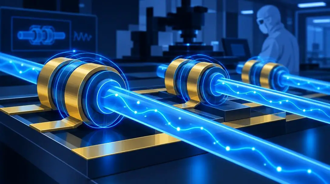
Nanowires are cylindrical structures with diameters measured on the scale of nanometers and unconstrained lengths. When fashioned into field-effect transistors, nanowires provide exceptionally tight electrostatic control over the conductive channel. Because the gate electrode can wrap entirely around the ultra-thin wire, nanowire field-effect transistors suppress parasitic leakage currents far more effectively than planar silicon. This architecture facilitates quicker digital switching, reduces overall physical footprint, and permits elevated operational frequencies without runaway thermal penalties.
Graphene Transistors
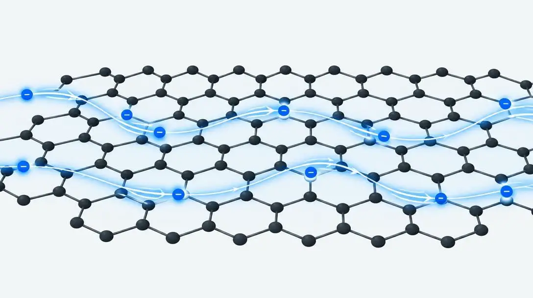
- Primary material: Single-layer hexagonal carbon lattice
- Key property: Ballistic electron mobility
- Target application: Ultrafast analog and digital signal processing
Composed of a two-dimensional sheet of carbon atoms arranged in a honeycomb pattern, graphene exhibits extraordinary electrical, thermal, and mechanical characteristics. Electrons travel through graphene with minimal resistance, a phenomenon often described as near-ballistic transport. Because electrical charges move across this atomic plane at tremendous velocities, graphene transistors can operate at frequencies far higher than conventional silicon gates, opening pathways to ultrafast processors that produce minimal internal friction and heat.
Spintronics Architecture
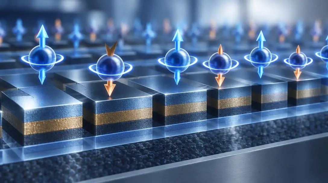
- Primary material: Ferromagnetic and non-magnetic nanoscale layers
- Key property: Electron spin state manipulation
- Target application: Non-volatile memory and ultra-low-power logic
Conventional computing relies strictly on the physical movement and presence of an electron's electrical charge to represent data. In contrast, spintronics (spin electronics) harnesses the intrinsic angular momentum, or magnetic spin orientation, of individual electrons. By orienting an electron's spin to point "up" or "down," spintronic components create non-volatile computational states that persist even when power is turned off. This technique eliminates standby energy leakage, dramatically boosts memory storage density, and accelerates write cycles.
Biomolecular Nanocomputers

- Primary material: Synthetic DNA and specialized enzymes
- Key property: Biochemical information encoding
- Target application: In vivo diagnostic sensing and targeted therapeutics
Rather than relying on solid-state electronics, biomolecular nanocomputers use biological molecules like deoxyribonucleic acid (DNA) to store and process complex data. DNA molecules can encode information within their nucleotide sequences, processing massive datasets in parallel through chemical binding reactions. Because these computational mechanisms operate in aqueous, biological environments, biomolecular computers can function directly inside living tissues to analyze biomarkers and execute real-time therapeutic responses.
| Technology | Core Mechanism | Primary Advantage | Key Research Focus |
|---|---|---|---|
| Nanowire Transistors | Surrounding-gate electrostatic control | Suppresses current leakage at small geometries | High-speed logic circuitry |
| Graphene Transistors | Two-dimensional ballistic electron transport | Exceptional carrier mobility and thermal conductivity | Ultrafast signal switching |
| Spintronics | Magnetic spin orientation (up/down) | Non-volatile state retention with zero idle power | High-density storage and cache |
| Biomolecular Computers | Nucleotide base-pairing and biochemical reactions | Massive parallelism in physiological environments | In vivo medical diagnostics |
Step-by-step: Integrating nanotechnology into computing systems
Transitioning from conceptual cleanroom prototypes to production-ready computing architectures requires a structured, multi-disciplinary engineering framework. Organizations pursuing nanoscale integration must address foundational physics, manufacturing precision, and legacy compatibility.
- Evaluate processing and architectural bottlenecks: Assess the existing processing pipeline to identify whether the primary performance constraint stems from thermal throttling, interconnect delay, or memory read/write latency.
- Select appropriate nanomaterials: Match the targeted computing bottleneck with the optimal material system. Deploy graphene or carbon nanotubes for high-velocity switching channels, spintronic nanomagnets for dense non-volatile storage, or nanophotonic guides to accelerate cross-chip bus communications.
- Refine nanoscale fabrication protocols: Establish advanced cleanroom manufacturing workflows capable of consistent 1-to-100 nanometer tolerance control. Implement extreme ultraviolet lithography, chemical vapor deposition, or directed molecular self-assembly depending on the physical structure of the selected material.
- Formulate hybrid integration plans: Engineer physical and electrical bridge interfaces that join nanoscale sub-components with conventional silicon circuitry and printed circuit board motherboards, ensuring compatible operational voltages and thermal expansion rates.
- Establish rigorous quality and testing frameworks: Construct automated diagnostic routines to scan for atomic dislocations, lattice flaws, and signal cross-talk across every manufactured die before final packaging and system deployment.
Pitfalls to avoid in nanoscale engineering
Developing hardware at atomic and molecular scales introduces operational variables that do not exist in conventional electronic fabrication. Avoiding common oversights ensures developmental resources yield functional hardware:
- Assuming macroscopic physics still applies: Treating nanoscale structures like miniaturized versions of macroscopic wires causes engineering failure. At these dimensions, quantum tunneling, surface interface resistance, and van der Waals forces dominate electron behavior.
- Overlooking manufacturing scalability: Fabricating a single pristine graphene transistor in a university laboratory is entirely different from patterning billions of identical switches across a commercial 300-millimeter wafer. Fabrication processes must emphasize repeatable throughput over bespoke perfection.
- Neglecting heat dissipation in high-density layouts: Although individual nanoscale components consume fractions of the energy required by silicon gates, packing trillions of them into dense three-dimensional blocks still produces localized heat pockets that demand careful thermal routing.
- Ignoring cross-compatibility with existing technologies: Developing a breakthrough nanoscale compute block that cannot interface with industry-standard operating systems, input/output buses, and logic levels guarantees commercial irrelevance.
- Disregarding contamination and environmental factors: Microscopic dust motes, ambient moisture, and minute electromagnetic variations can alter or destroy nanoscale circuits. Strict environmental isolation and defensive packaging are critical.
Overcoming fabrication, integration, and ethical hurdles
Despite its vast potential, the commercialization of nanoscale computing faces significant technical and societal roadblocks that require coordinated global solutions. Precision manufacturing remains the most immediate physical challenge. Placing individual carbon nanotubes or synthesizing defect-free single-atom graphene layers across large areas requires fabrication equipment operating at the edge of physical capability. A single atomic misalignment can render a logic gate useless, resulting in low manufacturing yields that drive production costs beyond commercial viability.
A second hurdle centers on hybrid integration. Silicon will not disappear overnight; rather, nanoscale components will initially operate as specialized co-processors and accelerators embedded within conventional silicon dies. However, bonding distinct materials such as carbon lattices, semiconductor nanowires, and biological compounds to silicon substrates presents severe chemical and thermal challenges. Differences in thermal expansion coefficients can cause layers to crack or delaminate under operational temperature swings, requiring the creation of entirely new bonding adhesives and interfacial metallurgical alloys.
Finally, researchers and industrial manufacturers must navigate serious ethical, health, and environmental concerns. The unique properties that make engineered nanoparticles useful—their microscopic dimensions and heightened chemical reactivity—also make them potentially hazardous if released into ecosystems or inhaled by fabrication workers. The life-cycle management of nanoscale computing components, from initial synthesis through cleanroom handling to electronic waste disposal, requires clear toxicological standards and responsible occupational safety protocols to prevent environmental contamination.
Strategic applications and future horizons
The successful scaling of nanotechnology will radiate across diverse industrial and humanitarian domains, solving computational problems that are fundamentally intractable for modern supercomputers.
In the realm of environmental sustainability, the adoption of ultra-low-power nanoscale processors can drastically curb the accelerating energy appetite of global data centers. Transitioning from leaking silicon gates to non-volatile spintronic storage and ballistically conductive graphene switches could reduce data processing power requirements by orders of magnitude, curbing the computing industry's collective carbon footprint.
In medicine and biotechnology, the convergence of computing and nanoscale biology promises to reshape healthcare. DNA-based nanocomputers and bio-compatible molecular sensors can travel through the vascular system, analyzing chemical concentrations in real time to locate cancerous cells or arterial plaques. Once a target is identified, these autonomous biological processors can trigger the localized release of therapeutic payloads, executing precision medicine with minimal systemic side effects.
Frequently asked questions
How small is the nanoscale used in modern computing research?
Nanotechnology in computing operates between 1 and 100 nanometers. At this tiny scale, individual devices are constructed from arrangements of individual atoms or molecules, allowing thousands of nanoscale elements to fit within the width of a single human hair.
Why are silicon computer chips reaching their physical limits?
As silicon transistors shrink toward the atomic level, classical physics no longer governs electron flow. Chips begin to suffer from quantum leakage currents, extreme thermal concentration, and material breakdown, preventing further performance gains through conventional scaling.
What is the difference between conventional computing and spintronics?
Conventional computing represents binary data solely through the presence or absence of an electrical charge. Spintronics utilizes the intrinsic magnetic spin orientation of electrons, enabling non-volatile memory that retains information without requiring continuous electrical power.
How can DNA and biomolecules function as computers?
Biomolecular nanocomputers use nucleotide sequences and enzyme reactions to encode and manipulate data. Because trillions of biological molecules can react simultaneously in an aqueous environment, they perform complex parallel calculations and operate directly inside living organisms.
Are nanomaterials already used in consumer products?
Yes. While advanced nanoscale computing processors remain primarily in research and specialized commercial development, nanomaterials are actively used today in products like antibacterial silver nanoparticle wound dressings and titanium dioxide sunscreens.
The bottom line
Nanotechnology represents a foundational departure from traditional semiconductor manufacturing, offering an engineering bridge past the physical barriers that constrain modern silicon chips. By exploiting the unique behaviors of matter at the 1-to-100 nanometer scale—from the rapid electron mobility of graphene to the zero-idle energy of spintronics—engineers are designing computing architectures that achieve unprecedented speed, density, and operational efficiency.
While substantial challenges remain in high-volume fabrication, silicon hybrid integration, and environmental safety governance, the technological imperative to move beyond silicon is absolute. As research labs refine cleanroom synthesis techniques and standardize characterization metrics, nanoscale computing will redefine consumer electronics, lower global digital power consumption, and unlock life-saving bio-computational frontiers.